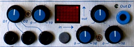
The Buchla 256e is a versitile control voltage processor.
|
|
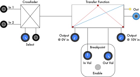
This is one section (out of four) from a Buchla 256e control voltage processor. The Transfer Function section is pretty unusual for a CV processor, and seems to confuse people at first, so I thought I would discuss it a little bit here. The Transfer Function has four knobs, a switch and the display. The leftmost knob and the three associated jacks area a CV crossfader, and are not part of the Transfer Function section.
|
|
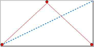
With the knobs as shown in this block diagram, whatever voltage is coming into the In2 jack is passed out of the crossfader to the Transfer Function section. The Transfer Function knobs describe a transfer that says that when the input voltage goes from 0 to 5 V, the output voltage will go from 0 to 10 V, then as the input voltage continues on from 5 to 10 V, the output voltages decreases from 10 to 0 V. |
|
|
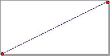
The blue dashed line represents the input to the Transfer Function, from 0 to 10.
|
|
If you picture a line connecting the LEDs, from left to right, in a 256e display, that defines an input->output Transfer Function. For example, if the left value is set to 0 and the right value is set to 10, as in this example, the input voltage will be passed to the output unchanged. |
|
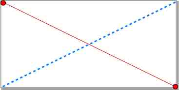
If the left value is 10, and the right value is 0, the input gets inverted.
|
|
If a breakpoint is added, the output gets to visit some exotic location defined by the XY position of the middle dot. In this example, a ramp from something like a 281 will be turned into a triangle. If you feed in a triangle, you will get a frequency-doubled triangle out. |